If there’s one thing leaders in Arizona wouldn’t be willing to trade, it’s the state’s grip on innovation.
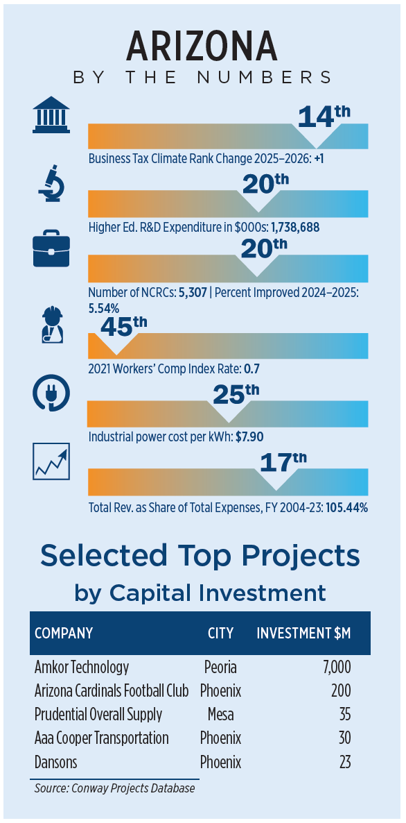
Beyond that, when it comes to global exports, trade has never been better. Arizona saw the second fastest export growth in the nation in 2025 with a $12 billion increase in exports over the prior year, a 37% jump.
Mexico by far represents the state’s top export destination, contributing $14.6 billion in 2025. The country came in well above the next top export destinations Taiwan ($4.5 billion), Canada ($2.8 billion), the Netherlands ($2.4 billion) and Germany ($1.6 billion). The leaderboard is quite symbiotic as the state’s 36% import increase last year was driven by goods from Taiwan ($16.7 billion), Mexico ($14 billion) and Canada ($2.8 billion).
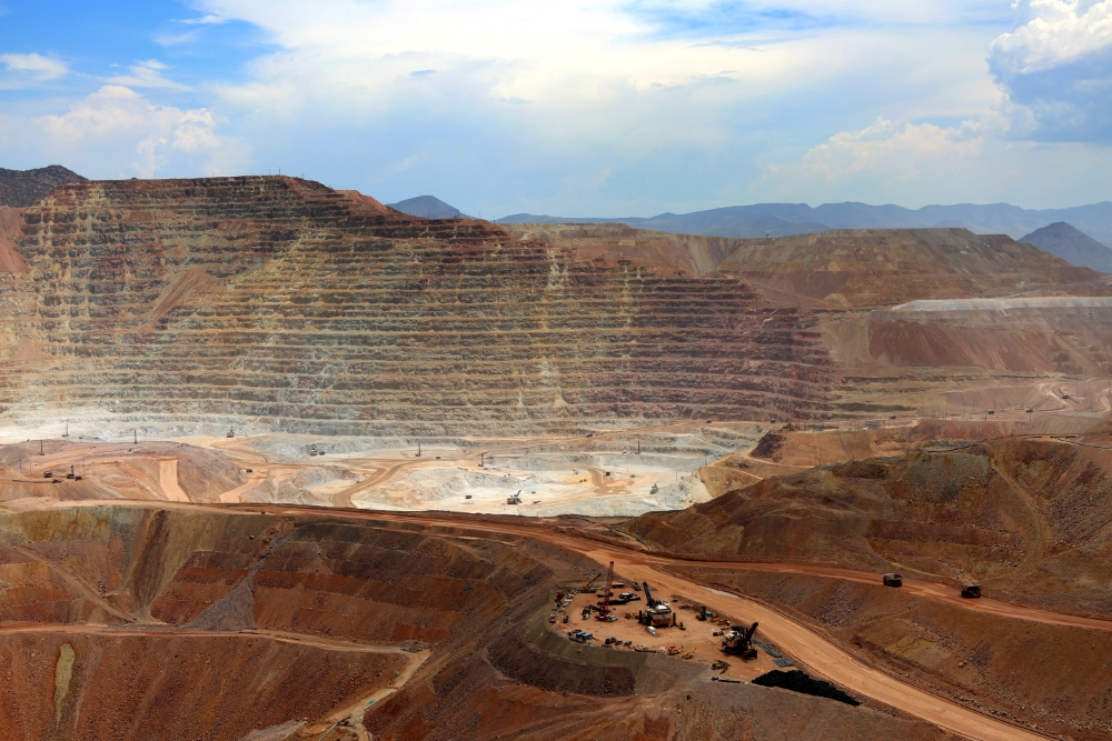
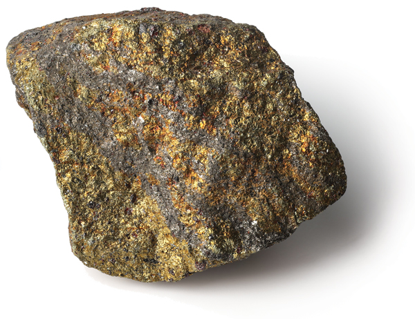
What are international partners sourcing from Arizona? The state is currently the No. 1 U.S. exporter of metal ores, coming in third for computer equipment, fifth for semiconductor and other electronic components, eighth for navigational, measuring, electromedical and control instruments, and rounding out the top 10 in the U.S. for aerospace parts and products.
Global markets are not only attracted to the state’s natural resources and roster of high-tech products — data shows interest has also been piqued for expanding international operations into Arizona. The state drew in over $195.7 billion in fresh international capital investment from 2020 to 2025, leading the nation during that period. Last year alone the state saw 55 foreign direct investment projects, pulling in 15 from Japan, 14 from Canada and seven from Taiwan.
Announcements included a $100 billion investment increase to Taiwan Semiconductor Manufacturing Company’s (TSMC) expansion activity in Phoenix, Japan-based Komatsu tripling its operational footprint in Mesa with a new mining facility and Canada-based Cyclic Materials’ over $20 million investment to establish its first rare earth elements recycling facility in Mesa. These projects helped the Phoenix-Mesa-Chandler metro earn Site Selection’s No. 1 metro rank in the Mountain region for the second year in a row in 2025 as the region attracted 84 major facility investments that qualified for Site Selection’s Conway Projects Database.
Arizona leaders are aiming to deliver on all fronts as new international operations find their stride. Whether it be formulating new avenues for global collaboration, refreshing research capabilities or targeted talent development alongside local industry, the state has been working behind the scenes to drive new opportunities forward.
I had the opportunity to catch up with Arizona Commerce Authority President and CEO Sandra Watson to discuss many of the forward-looking initiatives rolling out, particularly in Southern Arizona. Before we got there, however, we reflected on the monumental year.
Site Selection: Arizona saw a record-breaking year for exports in 2025, seeing the most growth (up 205%) in computer equipment. Do you expect that same demand this year? Are there any other industries where you anticipate heavy export growth?
Sandra Watson: We anticipate continued growth
in hightech exports, especially as semiconductor production and advanced electronics manu-facturing grow in Arizona. Beyond computer equipment, we’re seeing growth in aerospace components, electric vehicle technologies and renewable energy systems.
Site Selection: Aside from Mexico, Taiwan has emerged as a key trade partner for the state. What are Arizona’s top imports from the country? With a new MOU on the table, what excites you about unlocking potential FDI opportunities?
Watson: Arizona imports a significant amount of computer equipment and semiconductor-related equipment from Taiwan — ranking No. 1 among all states for imports from Taiwan. With the new MOU, there’s strong potential to deepen our collaboration in manufacturing capacity, and in R&D and workforce development. Taiwan’s semiconductor leadership paired with Arizona’s fast-growing ecosystem will support continued investment and high-tech growth.
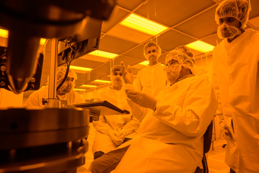
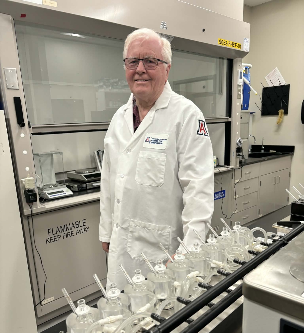
The NanoFabrication Core Facility’s cleanroom at the University of Arizona in Tucson grew from 2,800 sq. ft. to 6,800 sq. ft. as part of the over $35 million expansion project.
Photo courtesy of Kris Hanning, The University of Arizona Office of Research and Partnerships
Site Selection: Arizona has become the No. 1 U.S. state for international investment over the past five years. What has been Arizona’s marketing strategy, especially to countries without an existing FDI relationship?
Watson: Arizona’s international partners play a vital role in driving the state’s economic momentum. Arizona strengthens our global leadership by collaborating with international partners and countries in target growth markets.
Arizona has attracted record levels of international investment, driven by an emphasis on innovation, advanced manufacturing and long-term global engagement. To advance Arizona’s global competitiveness we established International Trade & Investment offices in Mexico, Canada, Europe, Israel, Taiwan, South Korea and Japan, which serve as platforms for cultivating economic collaboration and expanding the market reach of Arizona companies.
Between 2020 and 2025, Arizona landed 248 expansion projects from international companies, representing more than 55,000 potential new jobs and over $195 billion in investment — the most in the nation, according to fDi Markets.
Targeted Growth with Japan
Strategic international collaboration drove a freshly signed MOU involving the ACA, Greater Phoenix Economic Council (GPEC), Arizona State University and the Japan External Trade Organization (JETRO) in March 2026.
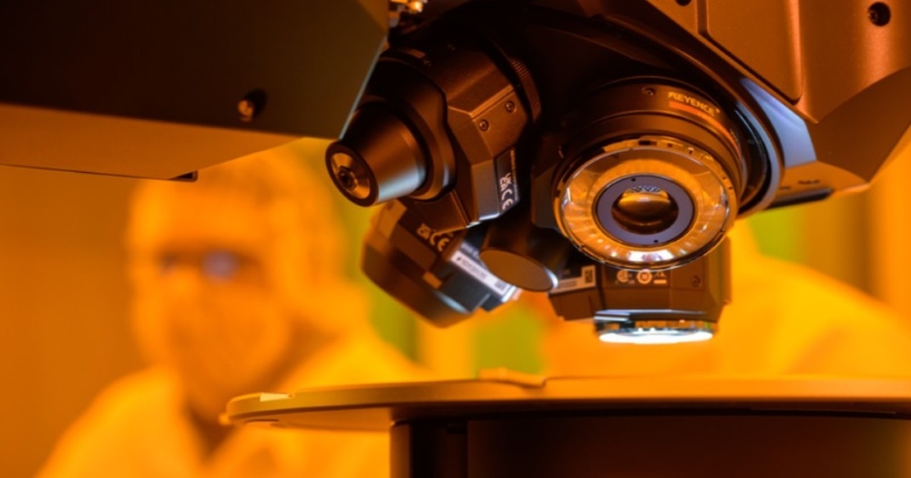
The expanded cleanroom and equipment additions better position NCF professors to pursue new research and support the needs of local companies.
Photo courtesy of Kris Hanning, The University of Arizona Office of Research and Partnerships
This partnership will focus on targeted industrial sectors including semiconductors, R&D and workforce development. Everyone is delivering something to the table in order to nurture industrial ecosystems in Arizona and Japan. A vital aspect of this initiative will be to connect regional industrial ecosystems in Japan to ASU’s research expertise and ACA and GPEC’s network of companies in the state.
Introductions to companies, educational institutions and local governments in Japan — and vice versa — through jointly coordinated events and programs aim to open doors to innovative technological exchange and human resource development.
Asked if this MOU is expected to drastically change the level of collaboration present from Japan in the state, or if this initiative will simply cement this long-term partnership on paper, Watson notes: “It does both. The MOU formalizes our already strong working relationship with JETRO, giving it a clear framework and shared priorities. At the same time, it opens new doors, sending a signal to companies and innovators in Japan that Arizona is committed to supporting new investment and strengthening collaboration.”
Over the past decade, the state has doubled its trade activity with Japan. In fact, last year the country became Arizona’s No. 1 source of foreign direct investment, committing 15 projects totaling $2.4 billion. In September 2025, the state launched its Trade and Investment Office in Japan with a goal of expanding its own international reach, while interacting with ecosystem players further downstream to open new opportunities for shared learning.
With that momentum rolling, Watson notes it was a pivotal moment to deepen collaboration with JETRO.
“What excites us most is the formal connection between two of the world’s most advanced technology hubs,” says Watson. “Arizona’s trade and investment relationship with Japan has grown significantly in recent years and as North America’s most advanced semiconductor cluster, we see tremendous opportunities to further expand partnerships that benefit both regions.”
But why not take it a step further? Exactly a week later, Arizona leaders were joined by officials from the City of Kaohsiung in Taiwan and the Kumamoto Prefecture in Japan to establish a trilateral MOU targeting semiconductors, R&D, workforce development and global supply chain integration. All players support key TSMC operations and are now joining forces to leverage strengths across semiconductor manufacturing, advanced packaging and research to unlock future innovation.
During Arizona Tech Week in April, ACA and Taiwan-based investor network Sustainable Impact Capital inked their own MOU as the duo look to establish the state as a national hub for Taiwanese companies and startups aiming to grow in the U.S. market.
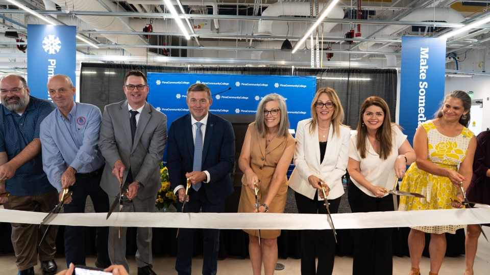
In March 2026, Governor Katie Hobbs (middle) and ACA President and CEO Sandra Watson joined Pima County Community College leaders in Tucson to launch the Advanced Manufacturing FIT Lab.
Photo courtesy of Office of Governor Katie Hobbs
Cleaning Up for Innovative Research
An estimated 28,000 new semiconductor-related jobs are projected to hit Arizona in the next several years, coming as a result of over 70 expansion projects totaling more than $214 in capital investment announced in the state since 2020.
Preparations for such activity became a key priority for the ACA, and not just in the Phoenix area. Three years ago, ACA announced a $35.5 million investment to more than double the NanoFabrication Core Facility (NFC) cleanroom at the University of Arizona in Tucson. NFC Director Dr. Greg Book says the former 2,800-sq.-ft. cleanroom, first delivered to the university’s Electrical and Computer Engineering Building in the late ’80s and early ’90s, had run its course.
It wasn’t a matter of starting completely fresh. Rather, the team moved to gut the entire cleanroom space, leaving only its walls and roof. Book says not even the flooring was spared, digging down an additional three feet in order to offer a raised floor cleanroom.
“That gave us a lot of flexibility with tool location and the size of the bays,” he says.
Upwards of $26 million of the funding went toward the expansion, bringing the cleanroom to 6,800 sq. ft., featuring a new metrology bay and overhauled infrastructure. Bays are where all processing happens and are the most critical environments in a cleanroom. In addition to metrology, the NFC processing capabilities cover photolithography, etching, chemical mechanical planarization, CVD, thermal oxidation & anneal and metallization — many of which are key to producing nanoscale technology.
“I was ecstatic,” he notes about first learning of the ACA’s dedicated funding. “The existing capabilities were not in a form that could support university research. The renovation breathed new life into the university for professors to be able to write new grants to pursue new research.”
A ribbon-cutting ceremony for the semiconductor cleanroom was held in February 2026. Book says with the expansion complete, the team’s focus now shifts to installation of tools. For current U of A students participating in a semiconductor processing class, this circumstance presented a unique opportunity to interact with advanced semiconductor technology.
“They are getting the chance to be here and help with this facilitation and tool installation. This is a real one-in-a-million, hands-on opportunity to take part in,” says Book. “It shows them what is involved in a fab startup and will be valuable to students who go on to work at, say, Intel or TSMC. They’re always building new fabs and that’s where they might get this opportunity again, but as a student, they wouldn’t get this really ever.”
Literal Tools from the Global Toolbox
The ability to learn about the tools while building them becomes an invaluable lesson in understanding the basic functionality of the equipment. In a future scenario, if an anomaly or outlier situation arises, talent would be more apt to know which component is the likely culprit. For a company, this awareness can make a major difference in length of downtime during production, which Book says could cost a fab upwards of $1 million for a single hour.
About $6 million of the funding was reserved for buying new state-of-the-art equipment to bolster the facility’s current assets. Book says new equipment came from around the world, providing the example of what he calls a “cluster tool” from Ontario-based Angstrom Engineering. It is one chamber under vacuum that can deposit up to eight different materials without breaking the vacuum. The equipment enables researchers dealing with very thin layers of material to avoid exposing various tools to the air and control surface chemistry.
Another tool brought in from the Netherlands will provide NFC the capabilities to enhance research for two-dimensional materials. For example, when working to pattern a device with graphene, researchers go through a process of putting on photoresist, exposing it, etching it or depositing it in an exposed area and then removing the photoresist. Depending on whether it’s silicon or carbon-based, removing it can run the risk of also removing the graphene. In this case, the new tool can remove the photoresist without touching the graphene.
Tucson-based optics company IRLabs donated an ultrasensitive infrared emissions microscope, capable of detecting chip failures before they happen. The addition of Apple Vision Pro and Meta Quest 3 headsets will allow students to explore the cleanroom and the equipment digitally to enhance their training.
Book states that as of now, the new cleanroom provides the NFC with an additional 3,000 sq. ft. to grow into. Outside of internal research conducted by U of A professors, the NFC additionally supports research for local companies and the U.S. Air Force. This includes research activity from a number of optical device companies and quantum device companies in the region, who require the same equipment to fabricate. In other cases, small companies run their entire businesses from NCF, utilizing multimillion-dollar cleanroom equipment to produce products on a fee-for-service basis.
“The cleanroom is very vital now to the state of Arizona,” says Book. “This renovation is enabling us to reach out to the semiconductor companies. We’re creating partnerships with TSMC in particular to help with workforce development, so that they can have a pipeline of new workers for the huge fab facility they’re building.”
He says the hope is to give U of A students an easier avenue to get in front of companies like TSMC or Intel, while developing new programs and classes that arm talent with the skills demanded for these evolving operations.
Strengthening Southern Arizona
About 20 minutes south of U of A’s campus, Pima Community College (PCC) is also modernizing its approach to workforce development, with a specific focus on advanced manufacturing.
PCC leaders were joined by Governor Katie Hobbs, the ACA, the City of Tucson, Pima County and local industry leaders in March 2026 to launch the state’s latest Future48 Workforce Accelerator. It marked the official opening of a 10,000-sq.-ft. Flexible Industry Training (FIT) Lab, housed within the campus’ Advanced Manufacturing Building.
“Southern Arizona’s economic future depends on our ability to prepare talent for rapidly changing industries,” said PCC Chancellor Dr. Jeffrey P. Nasse. “The FIT Lab gives Pima the ability to deliver flexible, market-driven training using the same advanced technologies found in advanced manufacturing. It furthers the college’s position as the region’s leading provider of workforce development and strengthens Arizona’s competitiveness in advanced industry.”
Introduction of the new FIT Lab was supported by a $3.2 million investment from the ACA in an effort to expand innovative opportunities for talent to gain industry-related skills, prioritizing a hands-on training experience. American Battery Factory is one local industry leader joining the mix to formulate new programs alongside PCC to support workforce needs at the company’s nearby manufacturing site.
Customized training programs look to tackle workforce demands across automation, robotics and smart manufacturing utilizing the exact tools and technology found on production floors. Unlike PCC’s typical manufacturing-focused programs, the FIT Lab will offer its courses regardless of the college’s semester schedules, enabling streamlined skills development.
The opening of PCC’s Future48 Accelerator comes after a year of targeted rollouts or announcements of other training centers in the state. In September 2025, Mohave College in Kingman celebrated the opening of its 36,000-sq.-ft. Advanced Manufacturing Training Center at the Kingman Airport Industrial Park. Unlike PCC, Mohave College’s Future48 Accelerator is preparing local students for careers including welding, HVAC, industrial maintenance, robotics, computer-aided drafting and manufacturing fundamentals. At the time of its launch, more than 65 students were enrolled in these programs.
Meanwhile, in Pinal County, employees of LG Energy Solution are helping lead Central Arizona College’s new battery manufacturing Future48 Accelerator. LG Energy’s Queen Creek battery manufacturing facility announced a construction halfway milestone in April 2025, as the company builds its first cylindrical battery plant in the nation. At Central Arizona College’s Superstition Mountain Campus the 19,850-sq.-ft. Accelerator will arm students with manufacturing skills specific to the production of cylindrical batteries.
LG’s involvement entails its current employees participating in hands-on training with manufacturing equipment that will be used at the facility. Ahead of its goal to hire 1,500 local employees by 2027, this groundwork arrived at the ideal time, complementing initiatives under Drive48, which was the first Future48 Accelerator program to launch in 2021. The automotive training assembly facility is also housed at Central Arizona College, allowing students to train alongside assembly robots. Prior to those launches, it was announced that Arizona Western Community College had broken ground on a new multi-purpose Future48 Workforce Accelerator in Yuma and Chandler-Gilber Community College in Mesa would gain an aerospace and defense-focused Accelerator.
I asked ACA’s Sandra Watson about the momentum driving the buildout of this workforce development infrastructure.
Site Selection: From U of A’s expanded cleanroom and Pima Community College’s new Flexible Industry Training Lab to a new MOU between Southern Arizona partners and Southern Taiwan, Tucson has become a key region for semiconductor and advanced manufacturing talent growth. Why has this region been pinpointed for these initiatives?

Sandra Watson, Arizona Commerce Authority President and CEO
Watson: The latest Future48 Workforce Accelerator, in partnership with Pima Community College providing battery and technology-focused training and the University of Arizona’s expanded semiconductor nano fabrication center, showcases Tucson’s leadership as a hub for advanced and cutting-edge technologies. Tucson’s education institutions, local government, growing workforce and innovation community provide an environment that helps business, startups and founders thrive. According to a 2025 study by CommericalCafe, Tucson ranked No. 5 for low labor and office costs, and growth of new businesses.
Four Future48 Workforce Accelerators were announced, broke ground or opened last year, and work behind the scenes stretches further. What can you tell me about the conversations that guided these facility placements?
Watson: The Future48 Workforce Accelerators are a nationally recognized workforce development program designed to scale talent quickly. The Accelerators are modeled after Drive48, an automotive assembly training facility in Pinal County that opened in 2021. A collaboration between the ACA, Central Arizona College, Pinal County, the City of Casa Grande and Lucid, Drive48 features multiple assembly robots and individual training rooms to prepare workers for jobs in automotive manufacturing.
The Future48 Workforce Accelerators are a network of advanced training facilities established in partnership with local community colleges in Tucson, Kingman, Yuma, Phoenix, Apache Junction, Casa Grande and Mesa.
The Accelerators provide hands-on training to prepare Arizonans for high-tech careers in manufacturing, battery, semiconductor, aerospace and defense and more.
For Drive48, ACA had extensive conversations about initiatives to provide hands-on training across high-growth sectors in collaboration with government and community colleges to meet the needs of industry.
The region’s semiconductor activity, bolstered by manufacturers like Intel, drew TOCALO to commit to Chandler.
Photo: Getty Images
Another Layer in Arizona’s Semiconductor Ecosystem
In April 2026, Japan-based TOCALO Co. announced plans to expand its global portfolio in Chandler by establishing a semiconductor coating services facility. The company selected the region for its deep industry ecosystem, skilled workforce and proximity to major U.S. transportation and technology corridors.
“We found Chandler’s environment and property to be perfectly aligned with our operational vision,” said TOCALO Global Business Development Headquarters Vice President Yasuki Nakahira.
The manufacturer specializes in advanced surface modification and coating technologies to support the semiconductor supply chain, locating in the region to better serve equipment providers and advanced manufacturing customers. TOCALO has leased an over 32,000-sq.-ft. facility for its new operations, which are expected to launch in 2027. This will be the manufacturer’s second U.S. facility, building upon current activity at its facility in La Palma, California.
“The addition of TOCALO further reinforces Chandler’s position within the global semiconductor supply chain,” said City of Chandler Economic Development Director Micah Miranda. “This investment supports high-precision manufacturing and aligns with the city’s strategy to attract advanced manufacturing companies that deliver long-term economic value.”
The investment comes at the same time that the Arizona Commerce Authority, Greater Phoenix Economic Council (GPEC), Arizona State University and the Japan External Trade Organization (JETRO) signed an MOU in March 2026 that among other goals focuses on targeted industrial sectors including semiconductors. — Alexis Elmore
Where Life Sciences Capabilities Grow
California-based life sciences company Arteris Bio announced plans to relocate to Arizona as the company looks to grow within the University of Arizona’s Tech Park in Tucson. The one-year-old company specializes in advanced topical technologies and is currently moving forward with its new topical platform, Redoxiv.
Arteris Bio Founder and CEO Dr. Bruce Register has a 30-year history ranging from working alongside startups to Fortune 500 life sciences companies, selecting the UA Tech Park for its cost-effectiveness and growing industry ecosystem to support his business.
“We chose to relocate from California to the UA Tech Park because it offers not only an exceptional environment for science-driven companies, but also a significantly more capital-efficient path for building and scaling a life sciences business,” said Register. “Its collaborative ecosystem and proximity to academic and clinical expertise make it an ideal setting as we advance our topical technology platform. This is about more than a single product — we are building a platform to unlock entirely new approaches to supporting both localized and potentially systemic physiological function through topical science.”
Dr. Bruce Register chose to move his life sciences company out of California to pursue new growth opportunities at the University of Arizona’s Tech Park in Tucson.
Photo courtesy of University of Arizona Tech Park
The platform is designed to keep skin healthy and comfortable, using a patented formulation of amino acid-based systems, bioactive cofactors and lipid-compatible delivery components that support physiological function, oxidative balance and skin barrier dynamics.
Arteris Bio moved into its 1,500-sq.-ft. lab and office at the Tech Park as of April 2026. Moving forward, the company aims to commercialize its operations at the Tech Park and scale infrastructure and partnerships that will drive future development and prepare the company for market entry. — Alexis Elmore