
by Akanksh Chandra Shekar, Senior Research Analyst, Tractus India
India’s chip plants are now shipping product. Kaynes reached commercial production 14 months after groundbreaking, well ahead of the typical 18 to 30 months for a greenfield assembly and test plant, according to IMARC Engineering.
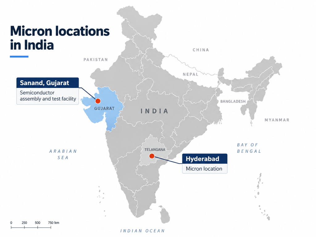
Three of the 12 approved manufacturing projects — Micron, Kaynes and CG Semi — are in commercial production, all in Sanand, Gujarat. At SEMICON India in September 2026, Prime Minister Narendra Modi said commercial production was also starting at two more plants, CDIL Semiconductor in Mohali, Punjab, and Suchi Semicon in Surat, Gujarat.
Semiconductors now sit at the center of how Asian governments compete for foreign direct investment, and every serious hub is backing its chip ambitions with public money. India joined that race later than most, so its progress is a fair test of whether a late mover can still build a credible position. The short answer is that scale is the wrong test for India. The question for investors is where in the chip value chain it fits, and on what timeline.
What India Has Committed
The 12 approved projects carry about US$17 billion of investment and cover one fab, two compound semiconductor fabs and nine packaging units, according to the Indian government, which offers fiscal support of up to 50% of project cost. On the design side, 24 projects are funded and 23 chip tapeouts (marking the transition from design to production) are complete.
In July, the Cabinet approved the second phase of the India Semiconductor Mission, ISM 2.0, with $13.25 billion across six pillars: design, equipment and materials, fabs, packaging, research and talent. The government expects five to eight more plants over the next seven to eight years. Project approvals under ISM 2.0 have not yet been announced.
What Is Being Built
India’s first fab, the Tata Electronics project in Dholera, Gujarat, is worth about $10.7 billion and is being built with Taiwan’s PSMC. Commercial production is now expected in mid-2028 rather than at the end of 2026, and it will start mainly on the older 90-nm. process, Angel One reported, citing Bloomberg. Located about 100 km. southwest of Ahmedabad, Dholera is touted as India’s first planned greenfield smart industrial city, with a focus on sustainability and advanced technology.
In Visakhapatnam, ASIP Technologies has started building a $300 million packaging plant with Korea’s APACT, targeting production within 18 months, EE Times reported. ASIP aims to reach 2.5D packaging by 2030.
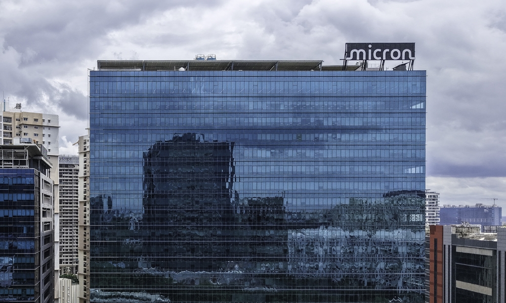
Micron’s Sanand plant assembles and tests DRAM and NAND memory chips for domestic and international markets. CG Semi’s Sanand plant assembles and tests chips for automobiles, scooters and industrial equipment, with exports to Japan, the United States and Europe. Kaynes Semicon packages chips using wire-bond and substrate-based formats.
Industry reporting by EE Times points to three gaps. The first is that India cannot yet package AI accelerators. The second is materials. Local sourcing of substrates, lead frames and mold compounds is zero today, with 20% to 30% expected in three to four years. The third is talent. Skills come largely from the Philippines, Malaysia and returning Indian engineers, and chip firms compete with the IT sector for staff.
In site searches for manufacturers across Indian states, the pattern is consistent. State packages are negotiated rather than read from a schedule, so two states with similar headline numbers can deliver very different outcomes once land terms, power tariffs, water allocation and the compliance burden of each park are priced in. Because materials have to be imported, inbound freight from Asian suppliers becomes a recurring cost line, and distance to port and customs handling weigh as heavily as the incentive itself. Each location needs to be tested on its own numbers rather than on the headline offer.
How Other Asian Ecosystems Compare
Taiwan is led by one company. TSMC raised its 2026 capital budget to between $60 billion and $64 billion, up from $52 billion to $56 billion. That is more than four times the whole ISM 2.0 outlay, spent by one firm in one year. The U.S. Department of Commerce said TSMC has committed a further $100 billion in Arizona, taking its planned U.S. investment to $265 billion.
South Korea backs scale with state support. In August it announced a $3.5 billion fund for materials, equipment and fabless chip design firms. Planned megaprojects worth about $246 billion are due to start building or expanding in 2026. The government plans to supply 14.7 GW of power to the Yongin cluster by 2041, and will launch a 10-year program worth about $700 million to link large chipmakers with smaller suppliers.
Japan concentrates its money on one company. Government support for Rapidus now totals about $14.8 billion after a further $4 billion in April, slightly more than India’s whole ISM 2.0 outlay. Rapidus is expected to need about $44 billion in total by fiscal 2031, with private investors and loans covering part of it. It targets 2-nm. mass production by 2027.
Malaysia is the closest comparison for packaging. Its semiconductor sector drew about $22.5 billion in approved investment from January 2024 to March 2026, $20 billion of it from foreign investors, according to The Edge Malaysia. The government has set aside $5.3 billion in fiscal support under its National Semiconductor Strategy, which aims to move the country from packaging and testing toward chip design and wafer making.
Vietnam is following a path similar to India’s: a late start, a first fab and visible state backing. Viettel broke ground on the country’s first fab on January 16, 2026. The 27-hectare (67-acre) site is at Hoa Lac near Hanoi, and Vietnam’s prime minister spoke at the ceremony. The plant will start at the 32-nm. node, with trial production due by the end of 2027 and process optimization through 2030.
The figures measure different things. India’s $17 billion is approved project investment, Malaysia’s figure is approved sector investment, Vietnam’s is cumulative foreign investment, and Taiwan’s is one firm’s yearly spending. Treat them as scale markers, not like-for-like comparisons.
What This Means for Investors
India cannot match Taiwan or South Korea on scale, and it does not need to. Its program is young, but it combines up to 50% fiscal support, a first fab under construction and plants already shipping chips. Vietnam, by comparison, has a first fab that is still about a year from trial production.
Four points follow. The first is to match the project to the stage. India suits backend packaging and testing of power, automotive and industrial chips today, alongside memory at Micron, while advanced AI packaging still belongs with Taiwan, South Korea or Malaysia.
The second is to plan for imported materials. With local supply at zero, lead time and duty matter more than wages.
The third is to watch the dates. Dholera is a 2028 story, Vietnam’s fab is a 2027 trial, and Rapidus targets 2027. The plants India has shipping today are packaging and testing plants, so that is where near-term supply deals sit.
The fourth is not to build a plan on ISM 2.0 funds until project approvals are announced.
The next test is simple. Can ISM 2.0 turn a few working plants into a cluster that has local suppliers, skilled people and advanced packaging?
Akanksh Chandra Shekar is a senior research analyst at Tractus India. Tractus (www.tractus-asia.com) is a leading Pan-Asia global site selection firm.