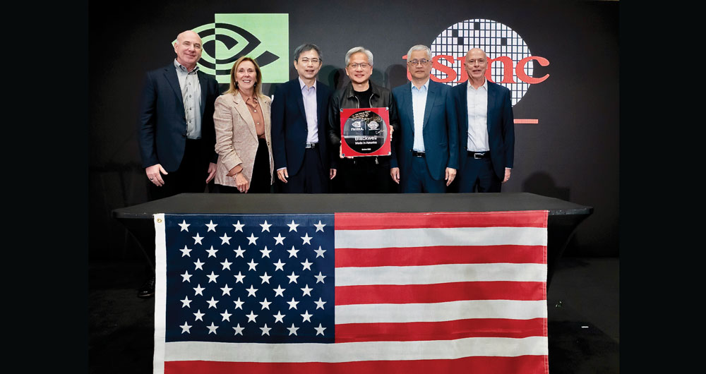
The spinoff from attracting semiconductor giant TSMC and its hundreds of billions of dollars of metro Phoenix investment is a case study for rainmaking in the desert. As the company’s supply chain began mapping its way to Greater Phoenix, some of the Taiwanese company’s suppliers need to be outside the denser urban areas. Before you knew it, those suppliers were landing like a flock of phoenixes, taking up sites in Casa Grande, Peoria, Chandler, Gilbert, Surprise, Mesa, Glendale and beyond.
International relations was part of Greater Phoenix Economic Council President and CEO Christine Mackay’s remit with the city before she joined GPEC this fall. She says the area’s lack of pedigrees and hierarchy lends itself to openness and welcome, not that there isn’t occasional pushback. She shares an anecdote from when TSMC brought in around 700 workers.
“A community member said we need them to hire American workers, not people from Taiwan,” she relates. “I said, ‘I love Starbucks, love a caramel macchiato, but I don’t know how to make one. For a year, they’re going to show me how, and at the end of a year, I will make macchiatos all day long.’ He said, ‘Oh. Okay.’ ”
The spinoff is cultural as well as logistical: The recent Double 10 celebration to honor Taiwan’s national holiday on October 10 drew 20,000 attendees for a night market, performances and fireworks in Glendale. Taiwan summer camp took place at Deer Valley Unified School District. And metro Phoenix continues to get a healthy amount of Arizona’s foreign direct investment, which has gone from 2% of the state’s business a decade ago to 35% today.
The industry has brought 100,000 jobs to the region over the past decade. Since 2020, Arizona has attracted more than 60 expansions in the semiconductor industry, representing roughly 25,000 projected new jobs and more than $205 billion in investment — more than any other state. Expanding companies have included Intel, TSMC, Amkor, Applied Materials, ASM, NXP, EMD Electronics, Benchmark Electronics, Sunlit Chemical, NRS Logistics, Pure Wafer, Edwards, Busch Vacuum, Pentagon Technologies and Fujifilm.
Let’s Get Together
It’s enough to make the entire international semiconductor industry want to convene in Phoenix too, just to find out what all the fuss is about.
October saw SEMICON West, the huge North American microelectronics exhibition and conference hosted by industry association SEMI in San Francisco for 50 years, land for the first time at Phoenix Convention Center, where the annual event will return in 2027 and 2029, alternating with the Bay Area. The event followed the region’s hosting of a SEMI conference on medtech led by MDM2, a GPEC-led medical device manufacturing consortium.
As 35,000 attendees and exhibitors rolled into town, I asked Joe Stockunas, president of SEMI Americas, why the event came and why the industry itself continues to thrive in metro Phoenix.
“Our decision to host SEMICON West 2025 in Phoenix marks a strategic shift for SEMI that aligns with so much investment in Arizona — now over $200 billion of announced investments in semiconductors — making Arizona a growing hub for manufacturing and technology innovation,” he explains. “The government and industry has also recently invested in workforce development, which is critical in addressing the talent gap facing our industry. There is strong local collaboration between public, private, government and academic entities. We have received great local support from the Arizona Commerce Authority, the Greater Phoenix Economic Council and Visit Phoenix, whose partnership has been instrumental in executing SEMICON West in Phoenix. And from the state level, we’ve had great support from Governor Katie Hobbs, who presented the opening keynote.”
The Phoenix Convention Center offered the exhibition space SEMI needed too, he says. “Hosting SEMICON West in Phoenix stands as a testament to the region’s achievements and future growth opportunities.”
Stockunas sees the potential for cross-sector innovation too.
“Semiconductors are the foundation of powering the technologies we rely on every day — from smartphones and computers to cars, medical devices and household appliances — keeping us connected and shaping how we live and work,” he says. “Investments in the semiconductor ecosystem and ensuring a robust and resilient supply chain has a downstream positive impact on other sectors such as MedTech and Mobility to power innovation in applications. SEMI has numerous technology communities focused on these key sectors, and we collaborate closely with companies in these spaces.”
When TSMC’s first investments were being made in Arizona, the company’s workforce challenges were well publicized. Asked for his perspective on how the state and region have responded, Stockunas says, “As the industry strives to achieve $1 trillion in revenue, ensuring we have the talent to support this goal is extremely critical, so workforce development is a key focus for the industry and it’s top of mind for SEMI and our member companies. Arizona has worked diligently to address the talent gap. There have been numerous investments in workforce development in the state to support training and apprenticeship programs. Arizona State University has risen to the rank of the largest engineering school in the country.”
SEMI in July announced it had partnered with Arizona State University to expand access to high-impact, on-demand training for the global semiconductor workforce. The newly launched courses, available through the SEMI University (SEMI U) learning platform, span emerging and foundational topics critical to today’s semiconductor professionals, including AI, packaging, process characterization, and operational excellence. The courses offer a certificate from ASU upon successful completion of each module.
Younger ages are on the radar too. In August, the SEMI Foundation, the nonprofit arm of SEMI, launched SEMIquest, an immersive, hands-on STEM experience on exhibition at the Arizona Science Center designed to “ignite curiosity and connect Arizona’s students to the vast career opportunities in the semiconductor industry.”
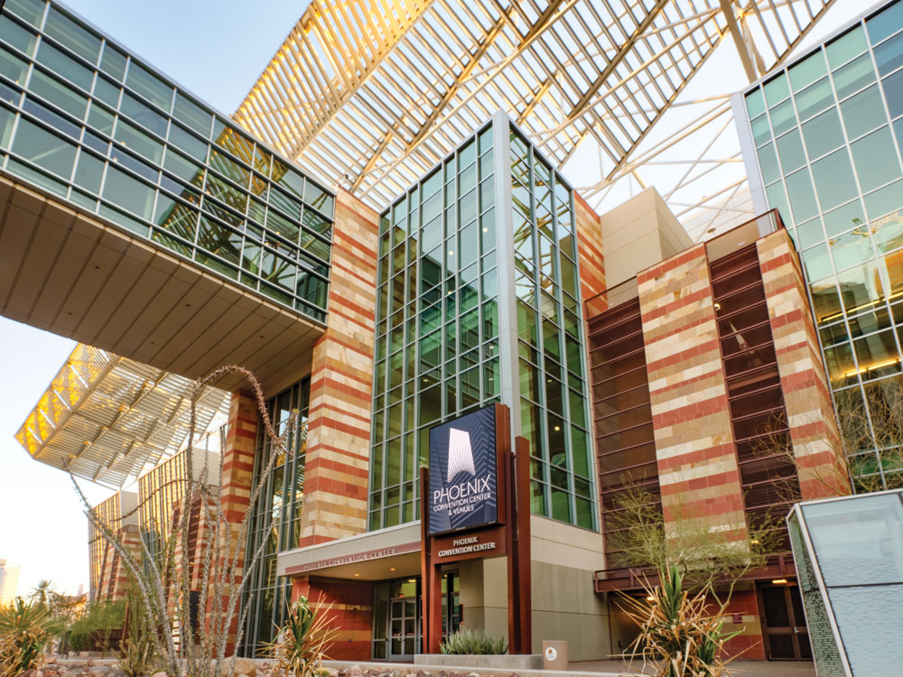
The SEMICON West event held at Phoenix Convention Center in October was the largest in 20 years, drawing an estimated 33% more attendees over last year. With more than 1,500 booths and 860 exhibiting companies, the event was projected to generate an estimated direct spend of nearly $10 million and more than 16,000 room nights.
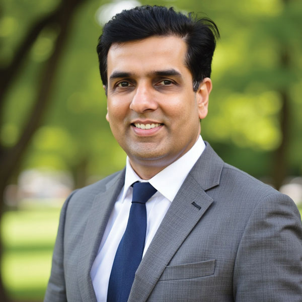
Naresh Naik, Director, SEMI University
After the conference was over, I connected with Naresh Naik, director of SEMI University, the organization’s education and training arm.
“SEMICON West’s debut in Phoenix clearly reinforced the region’s emergence as a global semiconductor hub,” Naik told me. “The event attracted record participation from equipment suppliers, materials companies and universities, all highlighting Arizona’s growing role in advanced manufacturing. The strong turnout from local talent, training institutions and workforce partners reflected a shared commitment to building a sustainable talent pipeline. SEMI University alone conducted eight in-person trainings with 270+ attendees and engaged hundreds more through its booth activities — a clear signal that the industry sees Greater Phoenix not just as a fab location, but as the center of a new semiconductor learning ecosystem.”
Could the showcasing of workforce programs give Greater Phoenix a leg up in the next competition? SEMI in mid-October announced the opening of the Regional Node Request for Proposals (RFP) for the National Network for Microelectronics Education (NNME), a national initiative funded by the U.S. National Science Foundation (NSF) to accelerate, expand, and improve microelectronics talent development across the United States. The SEMI Foundation serves as the NNME’s Hub Operator, and expects to support up to eight Regional Nodes, each with potential funding of up to $20 million over five years, to establish and share the gold standard for microelectronics education and workforce training across America. Proposals are due by December 22, 2025, and awards will be announced in early 2026.
Places and Projects
The conference allowed the city and region to highlight Foreign-Trade Zone (FTZ) No. 75. As Grantee, the City of Phoenix administers FTZ 75, which in 2023 reported over $22 billion in merchandise received and more than $3 billion in exports. “Semiconductor, aerospace and electronics firms actively leverage its benefits, from duty deferral and streamlined customs procedures to accelerated time-to-market, making Phoenix a powerful platform for global tech growth,” a city release explained, noting that among the area’s workforce-focused activities during the conference was a community of practice discussion at South Mountain Community College hosted by the Phoenix Workforce Coalition.
Prior to the conference, an Arizona delegation of more than 50 business, academia and community leaders led by the Arizona Commerce Authority traveled to Taiwan, where the delegation toured a TSMC training site, finalized new university partnerships, met with select businesses and took part in SEMICON Taiwan. “Afterwards, members of the group moved on to Japan for additional business meetings and to launch Arizona’s new Trade and Investment Office in Japan,” an ACA release explained.
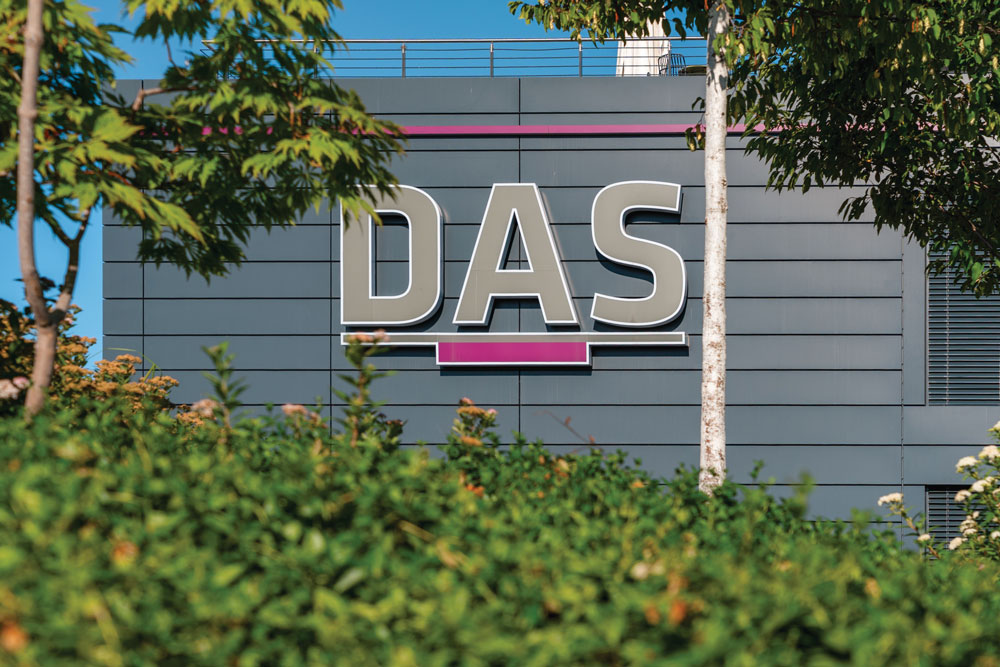
Germany’s DAS Environmental Experts Group, a major service and parts supplier to the semiconductor industry, in October opened a new Innovation & Support Center in Glendale.
CREDIT: Photo courtesy of DAS
As tens of thousands convened in Phoenix for SEMICON West, DAS Environmental Experts Group, a global provider of environmental technologies for waste gas and water treatment based in Dresden, Germany, opened a new Innovation & Support Center (ISC) in Glendale, an enlarged presence from its previous office in Phoenix, opened in 2022.
“The opening of our Glendale Innovation & Support Center is a clear signal of our commitment to the U.S. market,” said René Reichardt, CEO. “We are investing in Arizona and the U.S. workforce to ensure we can support customers locally with reliable service, spare parts availability and hands-on technical expertise. The facility’s tool training and classroom space provide real-world experience with a variety of DAS technologies, taking our customer care to a new level.”
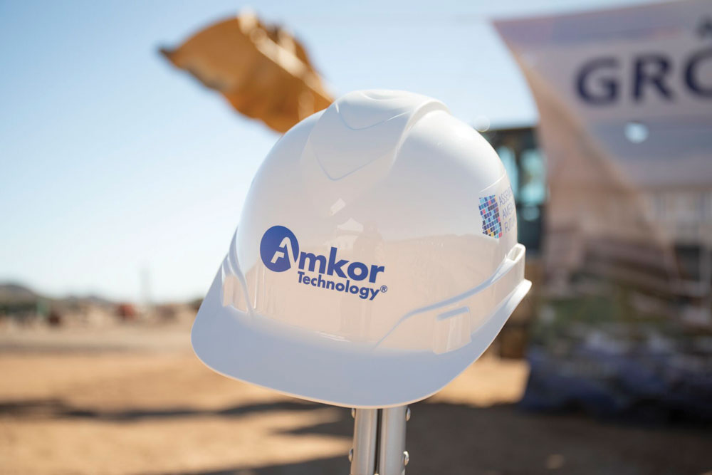
In October, Amkor broke ground on its Peoria semiconductor test and packaging facility and announced plans for a new expansion.
Photo courtesy of Amkor Technology
Dipping Into Arizona Chips
In October, Amkor Technologies officially broke ground on a $2 billion semiconductor advanced packaging and test site in Peoria, Arizona. Unlike most groundbreaking ceremonies, Amkor dug up excitement with news of an additional $5 billion investment into the facility.
Amkor increased the Arizona investment off the back of support from the Trump Administration’s CHIPS for America Program and the Advanced Manufacturing Investment Tax Credit. The funding boost will bring another construction phase to the project, which will include additional cleanroom space and a second greenfield packaging and test facility. With the initial phase in motion, Amkor anticipates its first manufacturing plant will be complete by mid-2027 and operational by the next year.
“This groundbreaking represents a bold step in Amkor’s long-term strategy for growth and innovation,” said Amkor President and CEO Giel Rutten. “We’re building a facility to meet our customers’ most advanced needs that will help shape the future of semiconductor manufacturing in the United States. Arizona offers the right mix of talent, infrastructure and industry presence, and we’re proud to deepen our roots here.”
In total, Amkor will house more than 750,000 sq. ft. of cleanroom space. The addition of another greenfield facility will allow the company to scale its advanced packaging capabilities to supply major customers such as Apple and NVIDIA, establishing the nation’s first high-volume advanced packaging facility. Semiconductors produced at the facility will be utilized within AI, automotive, mobile communications and high-performance computing applications.
“Factories across the United States are producing 19 billion chips for Apple this year alone, and Amkor’s new facility will package and test the Apple silicon produced at TSMC Arizona just down the road,” said Apple COO Sabih Khan. “We’re proud to invest in Amkor through Apple’s American Manufacturing Program, which is a key part of our $600 billion commitment to create jobs and accelerate innovation right here in the U.S.”
Production lines within the facilities will be scalable and equipped with smart factory technologies. Amkor’s facility will test and package Apple silicon produced at TSMC Arizona, only minutes down the road, as technology used at the site is designed to complement TSMC’s front-end wafer fabrication for full end-to-end semiconductor manufacturing. — Alexis Elmore